|
|
| PJRC.COM Offline Archive, February 07, 2004 Visit this page on the live site |
| ||
|
Shopping Cart
|
| Home | MP3 Player | 8051 Tools | All Projects | PJRC Store | Site Map |
|
You are here:
8051 Tools
| Search PJRC |
|
|
|
Each step is described briefly, with notes about areas that require special attention. A detailed procedure for testing the circuits added in each step is provided. No familiarity with PAULMON2 or 8051 assembly language programming is required to perform these tests (in order).
Though there is a lot of material presented here, the circuitry is designed and this material is arranged so that the construction can be accomplished easily in three steps. By performing the tests described here after each assembly step, the task of locating and correcting any problems is made as easy as possible.
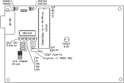
Most of the components require special attention. The diodes and electrolytic capacitors have a required polarity. The board will not work if they are inserted backwards, and the capacitors could be damaged. The notch on each chip should be aligned as shown in this picture:

Connect a five volt power supply to the board. The voltage must be between 4.5 to 5.5. The 12 volt input on the board is not required, and it's a good idea to leave it unconnected until it is needed.
Once the terminal program is running, turn on the power to the board. One or two random characters may appear on the computer's terminal window as the power is turned on. PAULMON2 waits for you to send a carriage return charactrer after the power is turned on (so it can detect your baud rate setting). Press Enter and you should receive the PAULMON2 welcome message:
               Welcome to PAULMON2 (beta7), by Paul Stoffregen

  See PAULMON2.DOC, PAULMON2.EQU and PAULMON2.HDR for more information.
If you do not get this message, then something isn't correct.
Add a web page about troubleshooting each stage of construction
and make a link from here to the troubleshooting section for
step #1.
Once you get the PAULMON2 message, feel free to explore the PAULMON2 menus and features. Some operations may have no effect until after the RAM chip is added in step #2, but the program should be able run correctly without any of the other chips that will be added in steps #2 and #3.
You may want to try increasing the baud rate, which requires turning the power off to the board, because PAULMON2 attempts to remember the baud rate so that it won't need to be auto-detected if you restart by pressing the reset button on the board. Using the 11.0592 MHz crystal, PAULMON2 should work correctly at 19200 and 57600 baud (the 8051 can not generate 38400 with this crystal). Many programs that run on a PC, particularily under MS Windows, can not reliably communicate at these speeds. Other crystals, even faster ones, may not be able to work at fast baud rates. See the Automatic Baud Rate Detection in the code library for more details.
When you're ready to begin solding again, proceed to the next step where you will gain the ability to download your own programs to the board and run them.
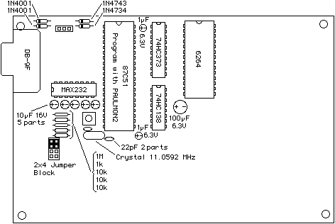
After these 3 chips are added, you will be able to download your own programs to the board. As PAULMON2 receives the data, it is writes it into the RAM chip. Of course, you can run your program once it's in the RAM chip, as well as make use of a number of other features of PAULMON2.

Begin ascii transfer of Intel hex file, or ESC to abort.
Then you must send the ex1_2.obj file to PAULMON2. Most terminal
emulation programs call this ASCII Upload or some similar name.
The text that appears on the screen should look like this:
PAULMON2 (beta7) Loc:2000 > Download

Begin ascii transfer of Intel hex file, or ESC to abort

.................................
Download completed

Summary:
 33  lines received
 505  bytes received
 505  bytes written
No errors detected
In most cases where the RAM is not working properly, an error about "Unable to write" should appear. Other types of errors, such as checksums, unexpected hex digits, etc usually indicate problems with the download process. If you do get any errors or the download process doesn't appear as shown above, go to the step #2 troubleshooting section.
It is important to download the EX1_2.OBJ file, because it is assembled beginning at memory location 2000 (hex). The EX1_4.OBJ and EX1_8.obj files are assembled at 4000 and 8000 (hex), for boards which have memory in those ranges. When the 28F256 chip is added in step #3, there will be memory from 8000 to FFFF, and you should be able to download EX1_8.OBJ to the 28F256 chip.
Once the program has downloaded sucessfully, you can run it with the JUMP command (press "J"). The memory location to jump to should be 2000, and it will probably be the default location.
The EX1_2.OBJ program will prompt you to enter a string. Here is an example when "PAULMON" is typed:
Please type a word (9 char max): PAULMON


######      #     ##   ##  ##       ##   ##   #####   ##   ##
#######    ###    ##   ##  ##       ### ###  #######  ###  ##
##   ##    ###    ##   ##  ##       #######  ##   ##  ###  ##
##   ##   ## ##   ##   ##  ##       ## # ##  ##   ##  #### ##
#######   ## ##   ##   ##  ##       ## # ##  ##   ##  ## # ##
######    #####   ##   ##  ##       ##   ##  ##   ##  ## ####
##       #######  ##   ##  ##       ##   ##  ##   ##  ##  ###
##       ##   ##  #######  #######  ##   ##  #######  ##   ##
##       ##   ##   #####   #######  ##   ##   #####   ##   ##


Press any key
If this message appears only briefly and then the system restarts, it is probably a sign that your terminal emulation software is configured to send CR/LF when you press Enter. If this is the case, it should be set to only send CR (ascii code 13).
At this point, you can download programs to your board. You may want to try writing a few simple programs, perhaps by copying and pasting bit of code from the EX1.ASM program. This program, like PAULMON and the examples in the code library, is in the public domain, so you can use whatever parts you find useful in your own programs. It may also be helpful to look over the PAULMON2 Documentation.
It won't be long until you'll want to have additional features on your board, which are added in the last step.
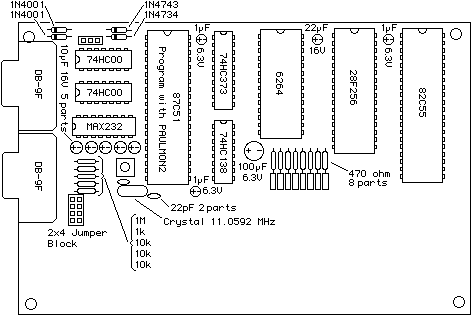
The 82C55 chip adds 24 I/O lines in three aditional ports. These ports are accessed differently that the 87C51's built-in ports, but they can be quite useful for controlling or communicating with other devices. A group of eight LEDs are connected to one of these additional ports. These can be useful for troubleshooting programs where it is not feasible to send troubleshooting data to the serial port (call to PHEX, COUT, etc).
The 28F256 adds 32k of additional space to store programs. The 28F256 is a non-volatile memory chip, so your programs will remain in the chip without power. PAULMON2 provides features to identify your programs, so it is possible to have PAULMON2 run your program automatically when the board is reset, so the board can be dedicated to a particular task after your code is working without reprogramming the 87C51. One of the jumper tells PAULMON2 to erase the 28F256 when the system is reset, in case you need to make changes to your code and download a new version. Of course, your program can also use portions of this chip for non-volatile data storage. PAULMON2 provides built-in routines your program can call to do the steps required to write/erase the chip.
The other serial port connector and the two 74HC00 chips provide another serial port. The 87C51 only has a single UART, so only one of these connectors can be in use at a time. However, many applications require the serial port for communication with some device other than a PC. When writing code for this sort of application, the first few lines would clear a port pin (P3.5) to switch the UART to the other connector, and perhaps change the baud rate and other serial communication parameters. If the board's reset pushed, the first serial port connecter will be used and PAULMON2 can be used to download a new verison of the code. This saves a lot of time and trouble switching serial cables every time the program is run, and it is possible to switch back and forth, such as briefly sending some troubleshooting data to the first serial port.
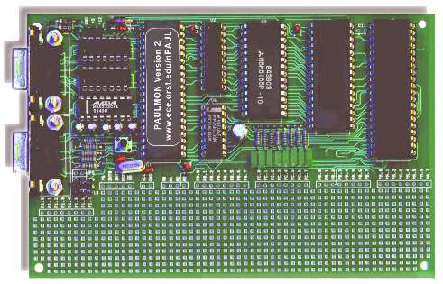
Each of these three sections functions independently and may be added when it is needed.

Describe how to check low voltage to see if resistor values are too low. Provide a second program which prompts for number to write to the port, and leaves it that way, to make testing the voltage easier.
28F256: download ex1_8.obj. Should work as before, but it will remain in memory after power goes out. Make sure to test the erase feature, with Menu in PAULMON2 and with the jumper. Should also provide a test program to download which illustrates how to use the flash rom for storing and retreiving and overwriting (pseudo-erase) data.
2nd Serial Port: download a (not yet available) test program... describe what the results should be. This program should do so interesting I/O on both ports, and illustrate the technique required to switch between them (waiting for TI bit).

Should create a web pages with example circuits and make a link to it from here. What should the examples be??