|
|
| PJRC.COM Offline Archive, February 07, 2004 Visit this page on the live site |
| ||
|
Shopping Cart
|
| Home | MP3 Player | 8051 Tools | All Projects | PJRC Store | Site Map |
|
You are here:
8051 Tools
| Search PJRC |
|
If you purchased the unassembled kit, the parts will come packaged into bags the correspond to these suggested assembly steps.
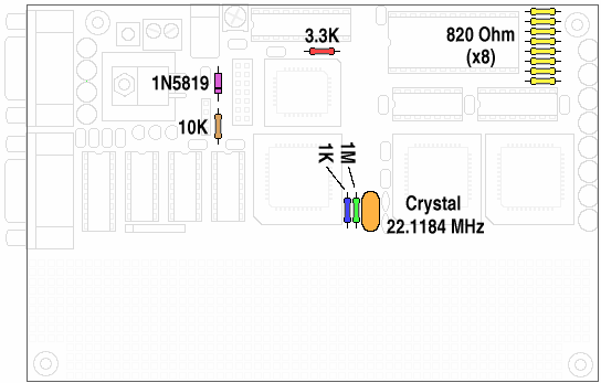 | |
| Figure 1: Step 1 - Low Profile Parts: Resistors, Diode and Crystal | |
| ||||||||||||||||||||||||
| Table 1: Parts List for Step 1 |
When soldering the 330 ohm resistor network, pin 1 must be aligned as shown in figure 2. Care should also be taken to verify that it is at approximately a 90 degree angle to the board, which is easiest to check and fix after only one of the six pins is soldered. If the resistor network is crooked, it can prevent placement of the 14 pin DIP sockets in step 3.
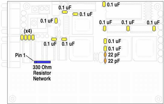 | |
| Figure 2: Step 2 - Short Parts: Capacitors and Resistor Network | |
| ||||||||||||
| Table 2: Parts List for Step 2 |
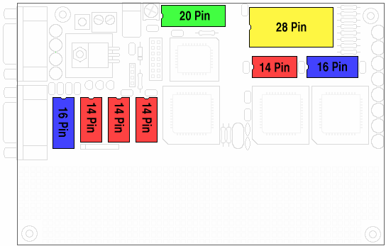 | |
| Figure 3: Step 3 - DIP Sockets | |
| |||||||||||||||
| Table 3: Parts List for Step 3 |
Likewise, the 4 pin header and 14 pin LCD socket should be checked carefully for proper alignment (easiest with 1 pin soldered).
The PLCC sockets must be oriented correctly, with their corner notches facing in the directions shown in figure 4. It can be very difficult to desolder a PLCC socket without damage to the board, so the orientation of these sockets should be doubled checked!
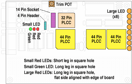 | |
| Figure 4: Step 4 - Medium Height Parts: PLCC Sockets, LEDs, Header, Socket, Trip Pot | |
| |||||||||||||||||||||||||||
| Table 4: Parts List for Step 4 |
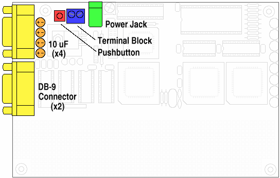 | |
| Figure 5: Step 5 - Tall Parts: Connectors, Pushbutton, Electrolytic Capacitors | |
| ||||||||||||||||||
| Table 5: Parts List for Step 5 |
If heatsink grease is available, a thin layer should be placed between the voltage regulator and heatsink to facilitate heat transfer. During normal operation, there is very little heating, but the heatsink allows the five volt power to be used for peripheral circuits you may later add in the prototype construction area, or for a LCD backlight.
The screw and nut should be used to secure the voltage regulator and heatsink to the board, so it remains still during soldering. Because to the thermal dissipation of the TO-220 package, a larger soldering iron tip should be used for better heat transfer.
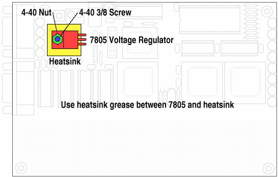 | |
| Figure 6: Step 6 - Voltage Regulator and Heatsink Assembly | |
| |||||||||||||||
| Table 6: Parts List for Step 6 |
DIP package parts are usually manufactured with their pins at a slight angle, so these will need to be straightened to fit into the sockets. All chips are polarity sensitive and must be inserted in the correct orientation.
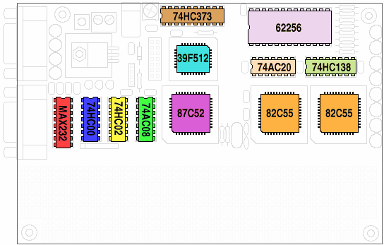 | |
| Figure 7: Step 7 - Install Chip Into Sockets | |
| ||||||||||||||||||||||||||||||||||||
| Table 7: Parts List for Step 7 |
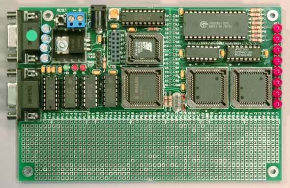
If a fancy "lab bench" power supply with built-in current limiting is not available, a good alternative is to connect a 47 to 100 ohm resistor in series with the positive lead of a +12 volt power supply. For example, if the board is shorted (one of the 74HCxx chips inserted backwards), a 100 ohm resistor will limit the current from 12 volts to only 120 mA. Keep in mind that the unregulated AC power adaptors that are rated for 12 volts will usually output higher voltage with light loading. 16 to 18 volts is common. A resistor of at least 100 ohms should be used in series with one of those power adaptors because of the higher output voltage.
The board should consume between 30 mA to 50 mA of current when no LCD is installed, no serial cable is connected, and only the green PWR LED is on. Monitor the current, either by connecting an amp meter in series, or by watching the current display on your power supply (if it has one), or by connecting a voltmeter accross the series resistor (if you are using a resistor to limit the current). If you observe excessive current, shut the power off immediately.
If you see zero current, the power may be connected in the wrong polarity, or the 1N5819 diode may be installed backwards or not soldered properly. Also check the 7805 voltage regulator connection.
As a final check before proceeding, measure the +5 volt power line on the board to verify that the 7805 voltage regulator is producing the proper +5 volt power for all the other chips on the board.
Apply power to the board again, after the terminal emulation program is running and has its baud rate and other settings established.
One or two random characters may appear on the computer's terminal window as the power is turned on. PAULMON2 waits for you to send a carriage return character after the power is turned on (so it can detect your baud rate setting). Press Enter and you should receive the PAULMON2 welcome message:
               Welcome to PAULMON2 v2.1, by Paul Stoffregen

  See PAULMON2.DOC, PAULMON2.EQU and PAULMON2.HDR for more information.


Program Name                     Location      Type
  List                             1000      External command
  Single-Step                      1400      External command
  Memory Editor (VT100)            1800      External command

PAULMON2 Loc:2000 >
|
If you did not receive this welcome message you pressed Enter, then it's time to start troubleshooting.
You will probably want to use the board at a faster baud rate. We suggest you select 115200 or 57600.
PAULMON2 stores the current baud rate information in the 8051's volatile internal RAM, so that it can skip the baud rate detection (waiting for you to press Enter) if the baud rate is already known. The downside to this is that you must remove power for a long enough time that the 8051's internal memory is cleared. Usually 5-10 seconds is enough time. When you restart from the power removed, PAULMON2 will wait for Enter to detect the baud rate. You must completely remove power each time you change the baud rate on the PC, so that PAULMON2 doesn't reboot and use the old baud rate while your PC is set to the new one (resulting in lots of "garbage" characters on the screen).
Begin ascii transfer of Intel hex file, or ESC to abort.
Then you must send the ex1_2.obj file to PAULMON2. Most terminal
emulation programs call this ASCII Upload or some similar name.
Hyperterminal uses "Send Text File..." in the "Transfer" menu.
The text that appears on the screen should look like this:
PAULMON2 Loc:2000 > Download Begin ascii transfer of Intel hex file, or ESC to abort ................................. Download completed Summary: 33 lines received 505 bytes received 505 bytes written No errors detected |
In most cases where the RAM is not working properly, an error about "Unable to write" should appear. Other types of errors, such as checksums, unexpected hex digits, etc usually indicate problems with the download process. If you do get any errors or the download process doesn't appear as shown above, go to the troubleshooting page.
In this example, EX1_2.OBJ was used. The other files are assembled at 4000 and 8000, which will use another part of the RAM or the Flash ROM. If you wish to try these, you will need to select their address to jump to them, instead of 2000 as shown.
Once the program has downloaded successfully, you can run it with the JUMP command (press "J"). The memory location to jump to should be 2000, and it will probably be the default location.
The EX1_2.OBJ program will prompt you to enter a string. Here is an example when "PAULMON" is typed:
Please type a word (9 char max): PAULMON ###### # ## ## ## ## ## ##### ## ## ####### ### ## ## ## ### ### ####### ### ## ## ## ### ## ## ## ####### ## ## ### ## ## ## ## ## ## ## ## ## # ## ## ## #### ## ####### ## ## ## ## ## ## # ## ## ## ## # ## ###### ##### ## ## ## ## ## ## ## ## #### ## ####### ## ## ## ## ## ## ## ## ### ## ## ## ####### ####### ## ## ####### ## ## ## ## ## ##### ####### ## ## ##### ## ## Press any key |
If this message appears only briefly and then the system restarts, it is probably a sign that your terminal emulation software is configured to send CR/LF when you press Enter. If this is the case, it should be set to only send CR (ascii code 13).
At this point, you can download programs to your board. You may want to try writing a few simple programs, perhaps by copying and pasting bit of code from the EX1.ASM program. This program, like PAULMON and the examples in the code library, is in the public domain, so you can use whatever parts you find useful in your own programs. It may also be helpful to look over the PAULMON2 Documentation.
The 82C55 chips and LEDs can be tested using the LED Blink example code, which is also available in C instead of assembly. These pages also illustrate the usage of the assembler and C compiler, which should get you started toward writing your own application using these languages.