|
|
| PJRC.COM Offline Archive, February 07, 2004 Visit this page on the live site |
| ||
|
Shopping Cart
|
| Home | MP3 Player | 8051 Tools | All Projects | PJRC Store | Site Map |
|
You are here:
MP3 Player
| Search PJRC |
 |
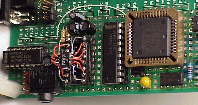
Well, at least the writing on the chips is somewhat readable. The Crystal CS4327 DAC only comes in the tiny SSOP package, which I soldered into a 16-pin DIP socket, as you can see here. It's a bit ugly, but it works ok for a prototype.
The TO-92 package part near the bottom of the MAS3507D is a 2N3904 NPN transistor, which is connected common emitter (to ground), with the base driven from P1.7, and the collector (with 3 volt pullup) connected to the decoder's reset line. The decoder has an active low reset, but the 8051's port pins default to high when it reboots. The yellow cap near the transisor is a 22 uF tantalum capacitor, which decouples the 3 volt supply. The line that runs along the bottom edge of the board is ground. To the right of the crystal is the LM317 voltage regulator, which makes 3 volts using a 220 ohm and 330 ohm resistor. The 330 ohm resistor isn't visible in these pictures. The resistors and capacitors just above the DAC are pairs of 3 ohm (1.5 ohm for each one, four resistors total), and the caps are 100 uF, 6.3 volt. These parts low-pass filter the 5 volt supply, for the DAC. The smaller cap, near the PSEN and INT1 pads, is a 1 uF required by the DAC. Two capacitors are located near the output jack (one is mostly hidden by the wires supporting the DAC in mid-air). These caps couple the DAC's output and remove the 2.5 volt offset. I really should have used opamps with a low-pass filter, as suggested by the DAC's datasheet... I'll certainly do that in the next design, but as it is it sounds quite good into a pair of amplified speakers.
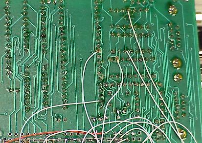
This picture may be helpful if you should try to make some sense out of the two wiring photos below. Don't forget to mentally flip it as you compare to the photos of the bottom side.
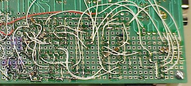
The MAS3507D gets its data from the 8051's serial port, operated in
mode 0 (clock sync serial, approx 1 MHz bit rate). There is one
trace cut on this board. Unfortunately the trace cut is near pin 11
of U7, which is the upper 14-pin chip (74HC00). The trace cut is
under the white wire that runs to that pin. This trace cut, and the
wire running down to the 74HC125 allows the serial port to receive
data in the normal way when the 8051's T0 line is high, the default
after a reboot, but when T0 is low, serial data reception is not
allowed. It's necessary to do this because the 8051's mode 0 needs
to turn the RXD pin into output to the MAS3507D, and having the
RXD pin driven by the NAND gate (or by a MAX232 for boards without
the serial port muxing gates) would cause a logic contention.