|
|
| PJRC.COM Offline Archive, February 07, 2004 Visit this page on the live site |
| ||
|
Shopping Cart
|
| Home | MP3 Player | 8051 Tools | All Projects | PJRC Store | Site Map |
|
You are here:
8051 Tools
| Search PJRC |
|
|
|
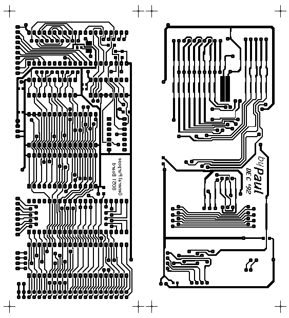
Here is a simple two sided pc board layout. This layout only makes connections to chips on the bottom side of the board, so sockets can easily be used in a hobbiest pc board that doesn't have plated through holes, like mine. How to make printed circuit boards is well beyond the scope of this document, of course.
 |
Several people have asked how to save images. Here's a few things to try.
Now you can also download a postscript copy of this layout, which should print out at the correct size. This postscript file includes a nice curve smoothing that unfortunately only works on an Apple LaserWriter, but it will print with jagged edges on other non-apple postscript printers.
These layout drawings must be printed at 100 dots per inch. They were drawn at this resolution in a pixel-based paint program, so these are the original artwork, not a low resolution copy. I use an Apple Laserwriter, which when used from the right Macintosh software applies a simple curve smoothing to the bitmap, which makes it look quite nice. It should work if printed without curve smoothing. One of these images must be flipped, since both are shown as a top view of the board.

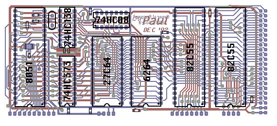
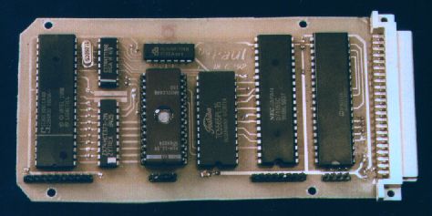
This simple diagram shows where to insert each chip. Be careful to get pin 1 aligned with the square pad for each chip. Surface mount capacitors are used for power supply decoupling. As well, two surface mount capacitors are used for the crystal oscillator. The third pair of pads near these is for a zero-ohm jumper. Near the center of the 8051 chip on the bottom of the board are surface mount pads for the reset capacitor and resistor. All the other surface mount pads are for decoupling capacitors. Care should be taken while mounting the crystal so that its metal case doesn't short to the traces which run underneath it. The two large rectangular pads, between the 74HC138 and 74HC373 are intended to reset the system when shorted with a metal object.

8051 Development Printed Circuit Board, component Side.

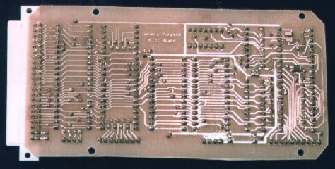
8051 Development Printed Circuit Board, Solder Side.
add layout for rs232 connector board with maxim chip on it.
The MAX232 and it's associated capacitors are mounted on a small circuit board which contains the 25 pin D-type connector.
An enlarged view of this section of the solder side of the board is available. Please contact me if you construct this board and you have trouble getting it to work.
![]() Go on to testing and getting it to work.
Go on to testing and getting it to work.