|
|
| PJRC.COM Offline Archive, February 07, 2004 Visit this page on the live site |
| ||
|
Shopping Cart
|
| Home | MP3 Player | 8051 Tools | All Projects | PJRC Store | Site Map |
|
You are here:
Printed Circuit Boards
| Search PJRC |
|
 Because this process does not support plate-through holes, you
need to make solder pads larger than they would be otherwise.
The minimum suggested size for a solder pad is 0.070 inches
diameter (7x7 pixels at 100 dpi). Traces should may be as
narrow at 0.01 inches (1 pixel at 100 dpi), but when space
permits traces should be at least 0.02 inches (2 pixels at 100 dpi).
When using a paint program, a template
image makes placing the components easy by using copy-n-paste.
Usually the easiest approach is to copy-n-paste all the component
pads (manually draw any unusual component pads), arrange them in
a way that seems to minimize routing for most of the signals,
place the printed image onto a piece of foam and stick all the
parts through the paper into the foam to check than you haven't
got two components sharing the same space. Finally connect all
the wires, typically with stick figures and once they're all
routed make it like nice.
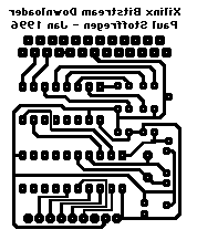
The image shown here is a simple single-sided board example. The
MIDI Drum Machine's board
is a good two-sided example, with a
solder side and
component side.
Note: the via pads on the MIDI Drum Machine board are smaller
than the suggested 70 pixel diameter... this caused considerable
trouble testing the board, since many of the vias did not
solder well. Before printing your layout, it is very helpful
to include some text and flip it if necessary so that it will
be readable when the image is positioned correctly. It's
not much fun to find out after etching that the layout image
had been placed on the board with the wrong side facing up.
Because this process does not support plate-through holes, you
need to make solder pads larger than they would be otherwise.
The minimum suggested size for a solder pad is 0.070 inches
diameter (7x7 pixels at 100 dpi). Traces should may be as
narrow at 0.01 inches (1 pixel at 100 dpi), but when space
permits traces should be at least 0.02 inches (2 pixels at 100 dpi).
When using a paint program, a template
image makes placing the components easy by using copy-n-paste.
Usually the easiest approach is to copy-n-paste all the component
pads (manually draw any unusual component pads), arrange them in
a way that seems to minimize routing for most of the signals,
place the printed image onto a piece of foam and stick all the
parts through the paper into the foam to check than you haven't
got two components sharing the same space. Finally connect all
the wires, typically with stick figures and once they're all
routed make it like nice.
The image shown here is a simple single-sided board example. The
MIDI Drum Machine's board
is a good two-sided example, with a
solder side and
component side.
Note: the via pads on the MIDI Drum Machine board are smaller
than the suggested 70 pixel diameter... this caused considerable
trouble testing the board, since many of the vias did not
solder well. Before printing your layout, it is very helpful
to include some text and flip it if necessary so that it will
be readable when the image is positioned correctly. It's
not much fun to find out after etching that the layout image
had been placed on the board with the wrong side facing up.